
- About making Printed Circuit boards -
On this page i try to describe howto make Printed Circuit boards from scratch. The process is not that complicated.
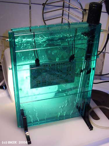
- VELLEMAN ET10 - Vertical etching tank -
This is the etching tank i use when making my own printed circuit boards for different projects. The tank is complete with heater and air-pump for liquid-agitation.
- Documentation -
Complete Users manual (In 37Kb .pdf file)
- The process -
-
The printed circuit board is made of fiberglass laminate with a thin layer of copper on one or both sides
(for single or double layer boards). I use PCB-Laminate material with pre-treated 'photo-resist' layer for
layout development using UV-Light.
- Make the PCB layout using 'PhotoShop' or other PC-Drawing software, or use ready made pcb-designs from magazines o.e.
- Transferee the PCB layout on to the 'Layout-mask', i use 100% transparent 'OH-Film' (Esselte 96011 for PCC photocopiers o.e.) and my laser printer or a Photo copying machine. I often use two printouts stapled togheter in order to get more 'Darkness' in the mask.
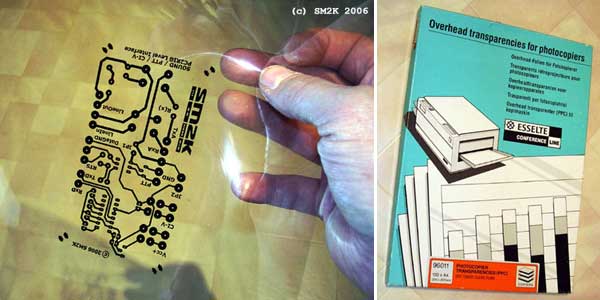
I use this the type of 'OH-Film' and my Laser printer to make the 'Layout-mask'
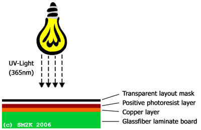
- Make the UV-Light exposure to Transferee the PCB layout onto the positive photo-resist treated copper-side on the laminate board, make sure you remove the protective cover from the laminate board, and that you turn the PCB layout 'OH-Film' the right way. When you 'look' from the direction of the UV-Light source the layout mask print text should read correctly (Not mirrored)
This is the 'normal' setup for the UV-Light expose.
In order to make the UV-Light Expose i use this HomeMade UV-Box. The wavelenght for the UV-Light is 365nm and the effect is 4x8W - Read more about the making of the HomeMade UV-Box --> Here!
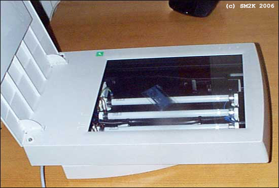
HomeMade UV-Box, using scrapped scanner case
- Process the UV-Light exposed laminate board in the 'development-fluid' to remove unwanted photo-resist.
- Wash the laminate board in wather.
- Process the laminate board in the etching fluid. Observe the process and stop when al unwanted copper is gone.
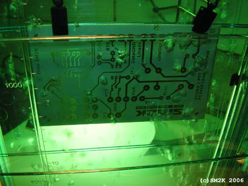
Processing a PCB in the tank, i use a 'backlight' for easy observation of the process
Observe carefully, and stop the process when al unwanted copper is gone...
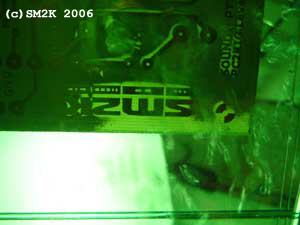
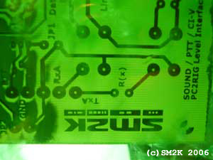
 Done!
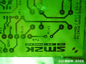
Done!
- Wash the laminate board in wather.
- Use soaped 'steel-wool' to clean the laminate board from remaining photo-resist.
- Let the laminate board dry.
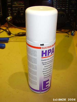
- Apply a layer of 'solder-safe' conformal coating. I Use 'Electrolube HPA' acrylic coating.
- Drill component holes, add components, solder and hawe fun!
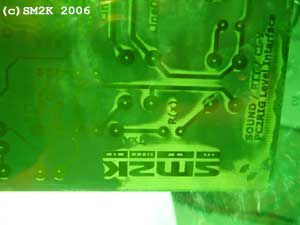
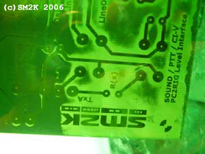
- DONE!
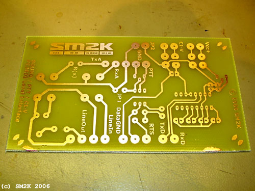
The printed circuit board ready to use!
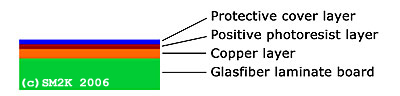
PCB-Laminate material wieved from the 'edge'
Protective cover layer - This layer is applyed at the factory to protect the 'photo-resist' layer. This layer is removed before exposing with UV-Light
Positive photo-resist layer - This is a thin layer of UV-Light sensitive coating. When this layer is exposed to UV-Light in the unwanted areas, the layer looses it hardening, and the unwanted areas is removed using development-fluid.
Copper layer - This is the copper layer that the will make the actual circuit. When etched the remaining photo-resist protects the areas that makes the circuit from the etching-fluid. Normal thickness of this layer is 17 to 35um.
Fiberglass laminate - Provides the structural integrity to the circuit board, other materials s.a. 'fenolpaper' or 'pertinax' my also be used.
This is the fluid mixture that i use when making PCB's


- Warning! Danger! -
The fluid's is dangerous if not properly used, always use rubber gloves and safety googles. When mixing the fluids always add the consentrate to the wather. DO NOT ADD WATHER TO THE CONSENTRATE!!! It might cause an uncontrolled reaction!
- Process time's -
This is the approximant time's that i use when making PCB's. The time's stated here is approximant because they can't be stated exactly. They depend mostly on fluid temperature and fluid mixture / age. The UV-Light exposure time and the photo resist development time also depend on the quality and age of the photo resist layer. The UV-Light exposure time also depend on the age of the UV-Lamp's used.
Go Back!
©1999-2006 SM2YER Goran